Important
I recommend that you read through every bullet point in this document; if I took the time to write it down here, there's a reason why.
These are my personal notes from taking EECS119 and using Cadence Virtuoso. The way most tutorials show you how to do it is bizarre, and not at all how the software is supposed to be used. I had to figure a lot of this out by trial and error, and wanted to save others the trouble for the future. This obviously doesn't cover everything and I'm still very much a beginner when it comes to using Cadence, but should be helpful for people also just starting out with VLSI design.
gl nerds 😎
-jmux
- Push
vfor vertical cursor in ADE visualization window - Directory for loading techfile on the EECS servers for EECS119 & EECS170C labs
- How to find the path of your home directory:
cd ~/ && pwd
- How to find the path of your home directory:
[YOUR HOME DIRECTORY]/eecs119/ncsu-cdk-1.6.0.beta/techfile
- Connect outputs of circut testbench to the
noConncomponent from thebasiclibrary. Eliminates DRC error about unconnected node.
Warning
Most importantly: Do DRC Regularly and NEVER do layout before testing that your schematic works
- Use wires (Not Rectangles) to connect components/instances:
ctrl+shift+w - Insert your custom components like normal components into the layout, and connect them by drawing onto their metal traces. As such, when you draw your inner components leave space at the end of the trace the pins are on to connect to.
- To view location of errors in Layout DRC: Verify -> Markers -> Find Markers
- LAYOUT EZ MODE
- From schematic, open LayoutXL
- In layout XL, go to bottom of screen and click on "generate all from source"
- LayoutXL will autogen pins, instances of nmos/cmos, and all you have to do is line them up
- To the right of that button, "Show/Hide incomplete nets" button. Select everything, and then click that to generate lines that go between the things you need to connect.
- See screenshots below for more information.
- One issue with generating from source is it sometimes won't recognize that certain nodes on the circuit are connected, and will keep the lines between them alive even though they're connected.
- LVS help - "Check against source"
- Bottom row - green checkmark button. Extracts and checks against schematic, but highlights and tells you what's wrong. Doesn't get all errors, and can be tempermental.
- Create wire
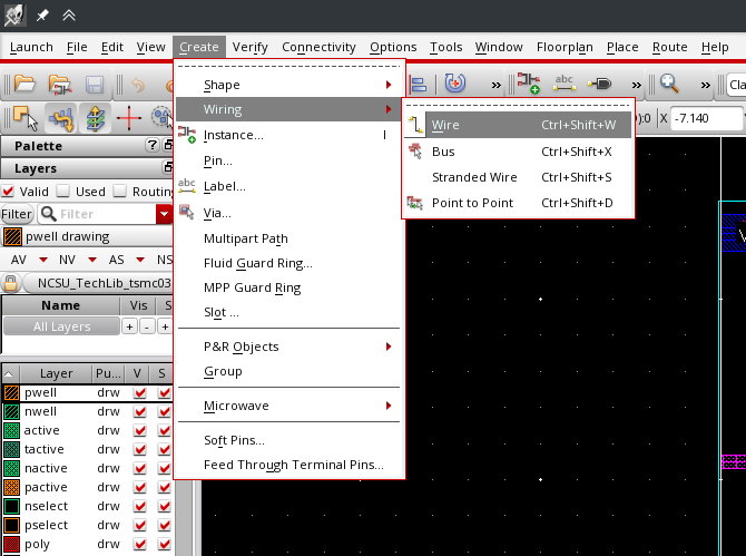
- Generate all from source
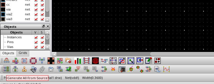
- Place components as in schematic
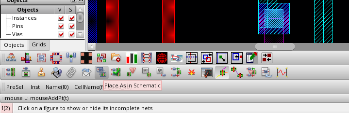
- Show/hide selected incomplete nets
- This is one of the most useful options in LayoutXL. It creates a ratsnest between your traces similar to how PCB layout works, making connecting your components much easier.

- Layout showing NAND gates placed as components in a standard cell layout, with wires going between them.
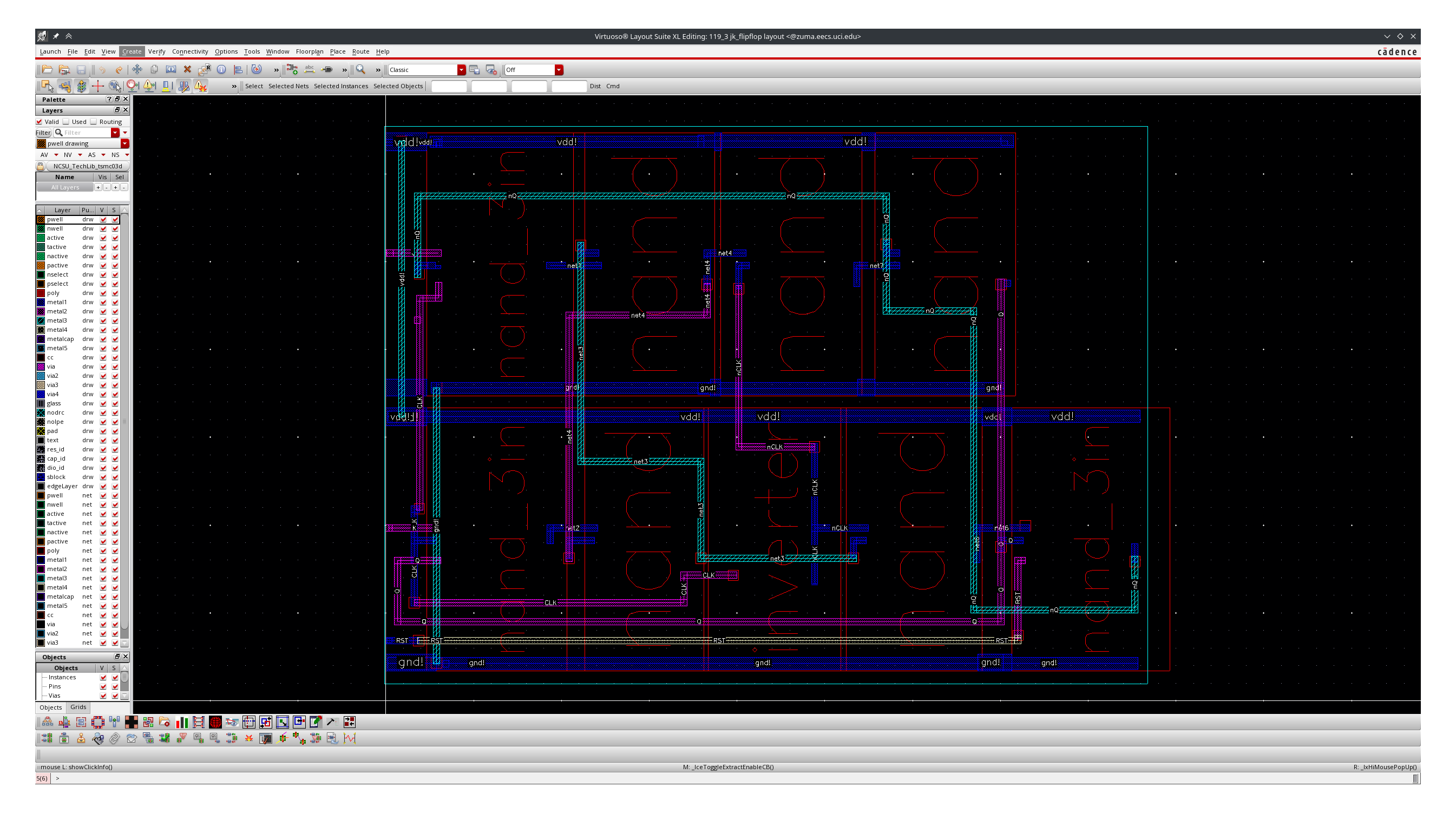
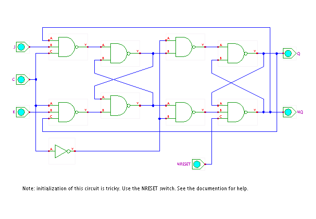
- 3 input JK Flip-flop (used in EECS119 HW3)
- fish
