The low-power STM8L family has the LSE (Low Speed External) oscillator that uses a 32.768kHz crystal to clock peripherals like the RTC. For my experiments I use the nrf24stm8l board I made some time ago: it's basically a STM8L051F3P6 breakout board with an nRF24L01 module header and a clock crystal:
Not all of the 20 MCU pins are broken out (it uses PC5/PC6 for the crystal and PB2/PB4 for the nRF24L01 header). A chip on a standard "green 10c TSSOP20 breakout PCB" with a crystal soldered to pins 1 and 2 also works (caps were not needed when I tried it).
This write-up is based on all free software, and the compiler/interpreter runs on the STM8 chip.
The STM8L051F3 image from the STM8 eForth 2.2.26 release can be used for the experiments below. The e4thcom terminal program was connected to PA2/USART_TX and PA3/USART_RX with a generic USB-RS232-TTL dongle interface.
The clock section of RM0031 states that the LSE can be activated manually or automatically, i.e. when a peripheral like the RTC or BEEP gets configured to use it.
In order to get an idea of the behavior in "manual mode" I wrote the following code:
\res MCU: STM8L051
\res export CLK_REGCSR CLK_ECKCR

#require ]B!
#require ]B?

NVM
\ Low Speed External 32.768kHz clock

: lse.on
  [ 1 CLK_ECKCR  2 ]B!
;

: lse.off
  [ 0 CLK_ECKCR  2 ]B!
;

: .lse CR ." LSE is " ;

: lse.stat
  [ CLK_REGCSR 5 ]B? IF .lse ." powered down" THEN
  [ CLK_ECKCR  2 ]B? IF .lse ." on" THEN
  [ CLK_ECKCR  3 ]B? IF .lse ." ready" THEN
;
RAM
After loading the code with e4thcom the following session shows how the LSE can be controlled:
lse.stat
LSE is powered down ok
lse.on ok
lse.stat
LSE is on
LSE is ready ok
lse.off ok
lse.stat
LSE is powered down ok
It's useful to keep this code in the Flash ROM for the next tests. To prevent it from getting removed when typing RESET just load and run PERSIST.
The beeper peripheral ("BEEP") is a rather complicated looking timer unit for a simple feature: create a 1, 2 or 4kHz beep signal.

- the input clock is either LSI (38Khz) or LSE (32.768kHz) followed by
- a programmable clock divider from 2 to 32 (in steps of 1) followed by
- an output clock "selector" that is a divider by 2, 4 or 8 followed by
- the PA0/BEEP (which also happens to be SWIM).
It can, as it is, also produce other frequencies. When using the LSE the a range of frequencies is thus 8.192Khz downto 128Hz. Such an output might be useful for other purposes, e.g. a frequency controlled boost converter. I noticed that activating the beeper also serves as a nice audible demonstration of the crystal start-up, and hence for a critical crystal oscillator property: you'll notice the frequency for about 1s change when activating the beeper!
When activating the beeper peripheral with the LSE as a clock source it will start the LSE, no manual configuration necessary. The configuration is straightforward but one must not forget to activate the peripheral clock gate for the beeper (RM0031 chapter 23 doesn'tmention that!):
\res MCU: STM8L051
\res export CLK_PCKENR1 CLK_ICKCR CLK_CBEEPR
\res export BEEP_CSR1 BEEP_CSR2

#require ]B!
#require ]B?
#require ]C!

NVM

: beep.on
  [ 1 CLK_PCKENR1 6 ]B! \ Peripheral clock gating register BEEP
  [ 1 CLK_CBEEPR 2 ]B!  \ select clock - bit1:LSI,  bit2:LSE
  \ [ $10 BEEP_CSR2 ]C!   \ BEEPDIV
  \ [ 1 BEEP_CSR2 6 ]B!   \ BEEPSEL
  \ [ 1 BEEP_CSR2 5 ]B!   \ BEEPEN
  [ $70 BEEP_CSR2 ]C!   \ all at once
;

: beep.off
  [ 0 BEEP_CSR2 5 ]B!   \ BEEPEN
;

\ set BEEPDIV from 0..30 (2 to 32)
: beep.div ( n -- )
  31 AND BEEP_CSR2 C@ $E0 AND OR BEEP_CSR2 C!
;

: gate.beep.off ( -- )
  \ disables access to BEEP_CSR2, beep will continue!
  [ 0 CLK_PCKENR1 6 ]B!
;

: .beep CR ." BEEP" ;

: beep.stat
  [ CLK_CBEEPR 0 ]B? IF .beep ." SWBSY is on" THEN
  [ CLK_ICKCR  6 ]B? IF .beep ." AHALT is on" THEN
  [ CLK_CBEEPR 1 ]B? IF .beep ."  clock is LSI" THEN
  [ CLK_CBEEPR 2 ]B? IF .beep ."  clock is LSE" THEN
  [ BEEP_CSR1 0 ]B? IF .beep ." MSR is on" THEN
  [ BEEP_CSR2 5 ]B? IF .beep ." EN is on" THEN
  .beep ." DIV =" BEEP_CSR2 C@ $1F AND .
  .beep ." SEL =" BEEP_CSR2 C@ $40 / .
;

RAM
The words beep.on and beep.off are actually all that's needed. The following test assumes that the code in the "LSE manual controll" section is still loaded:
\ the chip was just went through a PA1/NRST reset
lse.stat
LSE is powered down ok
\ now let's start the beeper
beep.on ok
\ the beeper starts within 1s: at first quiet for approx 0.5s,
\ then a sound with increasing pitch that quickly stabilizes
\ let's check the beeper status
beep.stat
BEEP clock is LSE
BEEPEN is on
BEEPDIV = 16
BEEPSEL = 1 ok
\ let's check the LSE:
lse.stat
LSE is on
LSE is ready on
\ let's try to disable the LSE
lse.off ok
\ the beeper is still active!
lse.stat
LSE is ready ok
\ even if there is no "LSE is on" flag
This means that the clock domain has a sufficient amount of "magic" to allow for some good configuration mistakes.
Here is one:
beep.on ok
\ the beeper is active - let's try to switch off its clock gate:
gate.beep.off ok
\ the beeper is still active! - let's try to turn it off:
beep.off ok
\ nothing happens - it's still active! Let's start over:
beep.on ok
beep.off ok
\ finally silence
This means that the beeper clock gate doesn't actually influence the peripheral - it enables the control of the peripheral! There is no mention of that in RM0031 chapter 23.
The sequence of events for activating the beeper in 23.2.1, quite obviously, doesn't apply for the LSE and can be safely ignored.
The RTC in a STM8L "Low density" device like the STM8L051F3P6 is has the following structure:
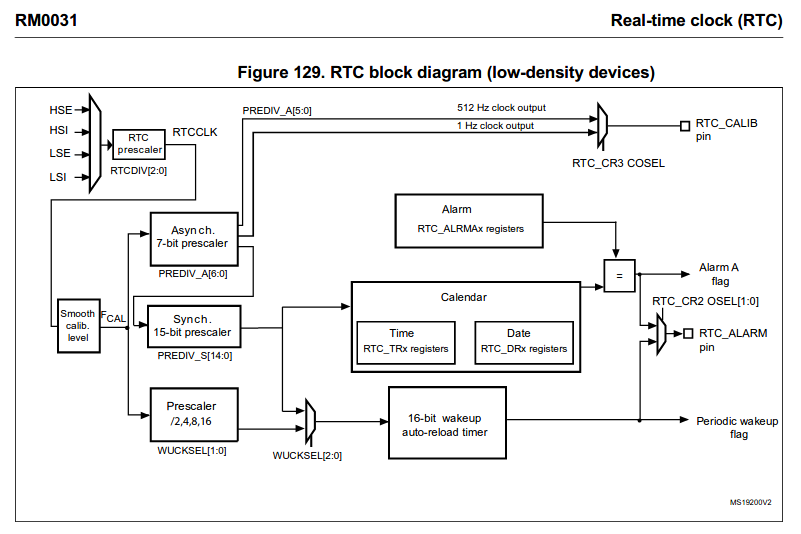
In order to be robust with respect to reset conditions the RTC configuration is split in two parts: one that controls the clock source and access to the RTC and the other that controls the RTC proper (configuration, prescalers, calendar and wakeup-timer). Unlike other peripherals only power-on reset will set the second part to default values.
Since the LSE works, in fact, with a 32.768kHz clock crystal the LSE clock source has to be selected with RTCSEL[3:0] in CLK_CRTCR. Since PREDIV_A is "1/128" and PREDIV_S is "1/256" by default (that is 1/32768) RTCDIV[2:0] needs to be set to "1/1".
After power-on, the RTC clock gate needs to be set-up once, and a clock source set-up inCLK_CRTCR has to be done (i.e. set RTCSEL to LSE and wait until the crystal oscillator has stabilized).
The RTC proper needs only be initialized after a power-on (i.e. after disconnecting/connecting the power supply). The RTC will even continue running while flashing the MCU!
It's not obvious from the specification but tests show that the clock source set-up in CLK_CRTCR isn't required when there was a reset other than power-on. For reading the RTC calendar the clock gate needs to be activated, that's all.
The following code shows the basic initialization of the RTC (without alarms or wakup-time):
\res MCU: STM8L051
\res export CLK_PCKENR2 CLK_CRTCR
\ \res export RTC_SPRERH RTC_SPRERL RTC_APRER
\res export RTC_WPR RTC_ISR1
\ \res export RTC_CR1 RTC_CR2 RTC_CR3
\res export RTC_DR1 RTC_DR2 RTC_DR3
\res export RTC_TR1 RTC_TR2 RTC_TR3

#require ]C!
#require ]B!
#require ]SPIN

: rtc.get ( -- s m h d m y )   \ read calendar
  \ RTC_TR1 and RTC_DR3 must be read in sequence
  RTC_TR1 C@  RTC_TR2 C@  RTC_TR3 C@  \ RTC_TR1: lock
  RTC_DR1 C@  RTC_DR2 C@  RTC_DR3 C@  \ RTC_DR1: unlock
;

: rtc.show ( -- )  \ show calendar
  rtc.get  ( s m h d m y )
  HEX
  CR ." Date:" . . .
  CR ." Time:" . . .
  DECIMAL
;

: rtc.gate ( -- )
  [ 1 CLK_PCKENR2 2 ]B!  \ peripheral clock gate RTC
;

: rtc.lse ( -- )  \ enable LSE and RTC clock gate
  \ rtc.gate  \ peripheral clock gate RTC
  [ $10 CLK_CRTCR ]C!    \ p.101 clock RTCDIV=1, RTCSEL:LSE
  [ 0 CLK_CRTCR 0 ]SPIN  \ p.101 RTCSWBSY set/reset by HW at clock change
;

: rtc.init ( -- )  \ initialize (and set) RTC
  \ rtc.lse  \ enable LSE clock

  \ 24.3.5 calendar initialization and configuration
  [ $CA  RTC_WPR ]C!     \ unlock calendar write protection
  [ $53  RTC_WPR ]C!

  [ 1 RTC_ISR1 7 ]B!     \ set INIT
  [ 1 RTC_ISR1 6 ]SPIN   \ wait until "INITF set"

  \ 24.3.1 set up clock (prescaler default: 1Hz @ 32.768kHz)
  \ [ $7F RTC_APRER ]C!    \ 24.6.16 PREDIV_A (default $7F)
  \ [ $00 RTC_SPRERH ]C!   \ 24.6.16 PREDIV_S (default $00)
  \ [ $FF RTC_SPRERL ]C!   \ 24.6.16 PREDIV_S (default $FF)

  \ [ 0 RTC_CR1 ]C!        \ 24.6.9 24h, Ratio>2x, no Bypass, WUCKSEL/16
  \ [ 0 RTC_CR2 ]C!        \ 24.6.10 no wakeup, no alarm
  \ [ 0 RTC_CR3 ]C!        \ 24.6.11 no output, no winter/summer time

  \ 24.3.5 calendar initialization and configuration
  [ $30 RTC_TR1 ]C!
  [ $20 RTC_TR2 ]C!
  [ $11 RTC_TR3 ]C!
  [ $28 RTC_DR1 ]C!
  [ $10 RTC_DR2 ]C!
  [ $20 RTC_DR3 ]C!

  [ 0 RTC_ISR1 7 ]B!     \ reset INIT
;
The following session shows the sequence after power-on:
rtc.gate ok
rtc.lse ok
rtc.init ok
rtc.show
Date: 20 10 28
Time: 11 20 34 ok
Note that leaving out either rtc.gate or rtc.lse after power-on reset will make the [ ... ]SPIN-lock in rtc.init hang.
The next session shows the behavior after the RTC was left running for about 15 minutes after a reset with the PA1/NRST pin:
rtc.show
Date: 0 21 1
Time: 0 0 0 ok
rtc.gate ok
rtc.show
Date: 20 10 28
Time: 11 34 56 ok
Reading the clock without activating the RTC clock gate with rtc.gate doesn't work. After setting the clock gate rtc.show displays the expected time, even though there was no new clock source set-up (CLK_CRTCR).
Depending on the robustness of the power supply designing a reliable system based on the STM8L RTC appears to be possible.
Initializing the WUT (Wakeup Timer) isn't difficult but a surprising number if peripheral register needs to be written (or checked).
The following examples produces WUT events at 2Hz, a rather high rate for this peripheral that can produce intervals as long as 36h. The configuration below uses RTCCLOCK at 32.768kHz, the WUT prescaler at "1/2" and the "16 bit wakeup auto-reload timer" at "1/8192". Without changing RTCCLOCK the lowest rate here is 0.25Hz.
By changing the WUCKSEL setting to using the 1s RTC clock the interval is up to 18.2h. A WUCKSEL setting with halt the RTC rate is also available.
\res MCU: STM8L051
\res export CLK_PCKENR2 CLK_CRTCR
\res export RTC_WPR RTC_ISR1 RTC_ISR2
\res export RTC_WUTRH RTC_WUTRL
\res export RTC_CR1 RTC_CR2 RTC_CR3
\res export PB_DDR PB_CR1

#require ]C!
#require ]B!
#require ]B?
#require ]SPIN

NVM

  : wut.init ( -- )   \ initialize (and set) WUT/RTC for PB3/RTC_ALARM
    \ enable LSE clock
    [ 1 CLK_PCKENR2 2 ]B!  \ peripheral clock gate RTC
    [ $10 CLK_CRTCR ]C!    \ p.101 clock RTCDIV=1, RTCSEL:LSE
    [ 0 CLK_CRTCR 0 ]SPIN  \ p.101 RTCSWBSY set/reset by HW at clock change

    \ 24.3.4 WUT initialization and configuration
    [ $CA  RTC_WPR ]C!     \ unlock calendar write protection
    [ $53  RTC_WPR ]C!

    \ 24.3.5 the clear WUTE-spinlock combination is certainly necessary
    [ 0 RTC_CR2 2 ]B!      \ 24.6.10 clear WUTE
    [ 1 RTC_ISR1 2 ]SPIN   \ 24.6.12 spin until WUT write is allowed
    [ $FF RTC_WUTRL ]C!    \ 24.6.18 wakeup timer register low  default: $FF
    [ $1F RTC_WUTRH ]C!    \ 24.6.17 wakeup timer register high default: $FF
    [ $03 RTC_CR1 ]C!      \ 24.6.9  WUCKSEL/2
    [ 1 RTC_CR2 2 ]B!      \ 24.6.10 set WUTE, enable WUT

    \ configure PB3/RTC_ALARM
    [ 1 PB_DDR 3 ]B!       \ enable output
    [ 1 PB_CR1 3 ]B!
    [ $60 RTC_CR3 ]C!      \ 24.6.11 OSEL:3 WUT output
  ;

  : wut.flag?  ( -- f )    \ get and reset WUTF
    [ RTC_ISR2 2 ]B?
    [ 0 RTC_ISR2 2 ]B!
  ;

RAM


\\ Example

#include stm8l-wut.fs

' wut.flag? BG !  \ make the output flash for 0 .. 5ms
wut.init
Note that the PB3/RTC_ALARM output is active until WUTF is cleared. This means that a software intervention is necessary in most use cases. A possible use case is running the MCU with a weak (high impedance) power supply and activate a low impedance supply just before waking up the MCU. Certainly this example is a bit far-fetched but right now I don't see other use cases for PB3/RTC_ALARM that can't be done with an interrupt routine and ordinary GPIO operations.
Surprisingly, the RTC in STM8L "Medium density" devices is inferior to that in "Low density" devices as it doesn't have the "Smooth calib. level" (RTC_SHIFTRx) or the RTC_SSRx sub-second features. STM8L "High density" devices have an additional "Tamper filter" feature but only the LQFP80 devices STM8L15xM8 STM8L162M8 and the LQFP64 decice STM8L162R8 seem to have it on pins. This feature might have applications in low power applications designed around the "Active Halt" mode, but that's not the issue here.
It may be possible to stubstitute the TIMx in the STM8 eForth with the "Wakup timer". That would have the advantage that "Active halt" can be used for applications when the console is not needed. Another application would be a BG like feature for the RTC "Alarm A" event. As it uses the same interrupt is the "Wakeup timer" the BG context could be used twice. A possible way for implementing that is refactoring the BG context switch code so that it can be replaced in STM8L applications.
There is an Application note AN3133 "Using the STM8L05xxx/STM8L101xx/STM8L15xxx/ STM8L162xx/STM8AL31xx/STM8AL3Lxx real-time clock" that explains some of the things in the RM0031 reference manual from another angle and explains e.g. clock calibration or tamper detection. It gets a few things wrong, though (e.g. there is no RTC in STM8L101 devices and RTC in STM8L "Low density" devices is alike that in "High density" devices.