This is a collection of code snippets for various features on the STM8S family microcontrollers (specifically the STM8S003F3). These are written against the STM8S/A SPL headers and compiled using SDCC.
Some of this controller's functions aren't particularly intuitive to program, so I'm dumping samples for future reference here. These are based on the STM8S documentation:
// Configure the clock for maximum speed on the 16MHz HSI oscillator
// At startup the clock output is divided by 8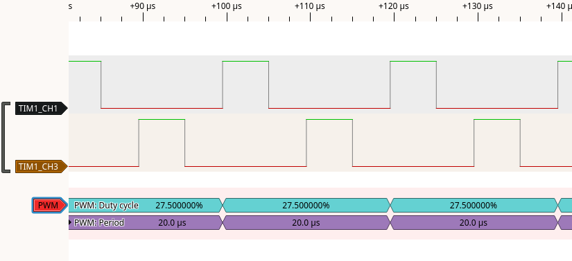
CLK->CKDIVR = 0x0;Note that on the STM8S003F3, TIM1_CH1 output requires configuring an Alternate Pin Function (see next snippet).
const uint16_t tim1_prescaler = 0;
TIM1->PSCRH = (tim1_prescaler >> 8);
TIM1->PSCRL = (tim1_prescaler & 0xFF);
const uint16_t tim1_auto_reload = 16000; // 1KHz assuming at 16MHz clock
TIM1->ARRH = (tim1_auto_reload >> 8);
TIM1->ARRL = (tim1_auto_reload & 0xFF);
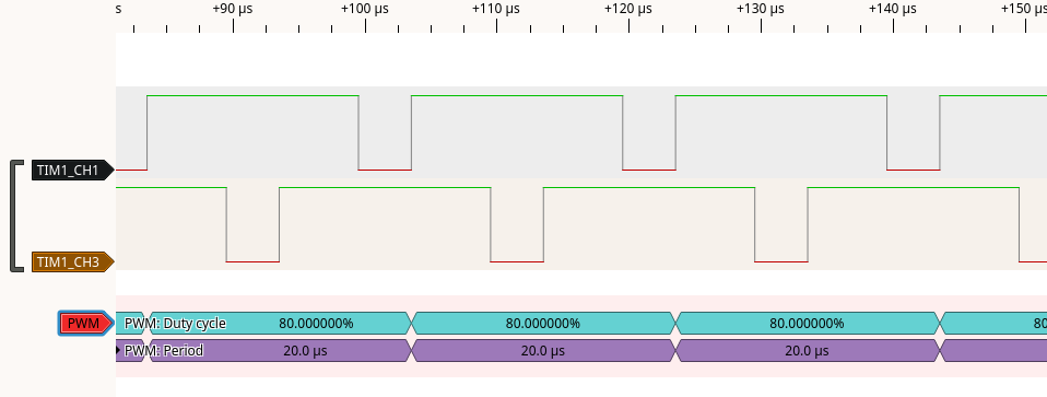
const uint16_t tim1_compare_reg1 = 4000; // 25% duty cycle
TIM1->CCR1H = (tim1_compare_reg1 >> 8);
TIM1->CCR1L = (tim1_compare_reg1 & 0xFF);
// Set up compare channel 1
TIM1->CCER1 = TIM1_CCER1_CC1E; // Enable compare channel 1 output
TIM1->CCMR1 = TIM1_OCMODE_PWM1; // Make OC1REF high when counter is less than CCR1 and low when higher
TIM1->EGR |= TIM1_EGR_UG; // Generate an update event to register new settings
TIM1->BKR = TIM1_BKR_MOE; // Enable TIM1 output channels
TIM1->CR1 = TIM1_CR1_CEN; // Enable the counterSome pins on the STM8S003 series are marked as having an "alternate function after remap". These are only documented in the datasheet, with register description under Option bytes.
As option bytes are stored in eeprom, they're a little more involved to set than regular registers. Eeprom can be addressed directly for reading, but needs to be unlocked before it can be written.
Option bytes are intended to be programmed once when uploading code to the chip, but they can be changed "on the fly" as the datasheet mentions:
// Set a bit in the Alternate Function Register (AFR) to switch pin-mapping
// This is stored in flash and is not a directly writable register
{
    const uint32_t AFR_DATA_ADDRESS = 0x4803;
    const uint32_t AFR_REQUIRED_VALUE = 0x1; // Enable TIM1_CH1 pin

    const uint16_t valueAndComplement = FLASH_ReadOptionByte(AFR_DATA_ADDRESS);
    const uint8_t currentValue = valueAndComplement >> 8;

    // Update value if the current option byte is corrupt or the wrong value
    if (valueAndComplement == 0 || currentValue != AFR_REQUIRED_VALUE) {
        FLASH_Unlock(FLASH_MEMTYPE_DATA);
        FLASH_ProgramOptionByte(AFR_DATA_ADDRESS, AFR_REQUIRED_VALUE);
        FLASH_Lock(FLASH_MEMTYPE_DATA);
    }
}
This works in a pinch and avoids an extra programming step, but switching function repeatedly during run-time is probably a bad idea:
-
There's likely an endurance issue as each change is written to flash/eeprom (datasheet claims 100k writes).
-
Writing some of the option bytes requires two writes: one for the data and one for its complement. If a reset occurs between the two writes, the option bytes need to be reprogrammed before the SWIM interface can program the chip again (stm8flash and ST Visual Programmer can still program the option bytes in this state, but error when trying to program the main flash).
// Set up ADC
ADC1->CSR |= ADC1_CHANNEL_4; // Select channel to read
ADC1->CR2 = ADC1_CR2_ALIGN; // Place LSB in lower register
ADC1->CR1 = ADC1_CR1_ADON; // Power on the ADC

// Trigger single conversion
// (Yes, you write a 1 to the register a second time to do this - super intuitive...)
ADC1->CR1 |= ADC1_CR1_ADON;

// Wait until conversion is done
while ((ADC1->CSR & ADC1_CSR_EOC) == 0);

// Clear done flag
ADC1->CSR &= ~ADC1_CSR_EOC;

// Load ADC reading (least-significant byte must be read first)
uint16_t result = ADC1->DRL;
result |= (ADC1->DRH << 8);This uses TIM1's compare channel 1 to trigger ADC readings. This can be slightly simpler if TRGO is configured to trigger on timer reset instead.
void init_adc(void)
{
    // Configure ADC to do conversion on timer 1's TRGO event
    ADC1->CSR = ADC1_CSR_EOCIE | // Enable interrupt at end of conversion
                ADC1_CHANNEL_4; // Convert on ADC channel 4 (pin D3)

    ADC1->CR2 = ADC1_CR2_ALIGN | // Place LSB in lower register
                ADC1_CR2_EXTTRIG; // Start conversion on external event (TIM1 TRGO event)

    ADC1->CR1 = ADC1_PRESSEL_FCPU_D18 | // ADC @ fcpu/18
                ADC1_CR1_ADON; // Power on the ADC


    // Configure TIM1 to trigger ADC conversion automatically
    const uint16_t tim1_prescaler = 16000; // Prescale the 16MHz system clock to a 1ms tick
    TIM1->PSCRH = (tim1_prescaler >> 8);
    TIM1->PSCRL = (tim1_prescaler & 0xFF);

    const uint16_t tim1_auto_reload = 69; // Number of milliseconds to count to
    TIM1->ARRH = (tim1_auto_reload >> 8);
    TIM1->ARRL = (tim1_auto_reload & 0xFF);

    const uint16_t tim1_compare_reg1 = 1; // Create a 1ms OC1REF pulse (PWM1 mode)
    TIM1->CCR1H = (tim1_compare_reg1 >> 8);
    TIM1->CCR1L = (tim1_compare_reg1 & 0xFF);

    // Use capture-compare channel 1 to trigger ADC conversions
    // This doesn't have any affect on pin outputs as TIM1_CCER1_CC1E and TIM1_BKR_MOE are not set
    TIM1->CCMR1 = TIM1_OCMODE_PWM1; // Make OC1REF high when counter is less than CCR1 and low when higher
    TIM1->EGR = TIM1_EGR_CC1G; // Enable compare register 1 event
    TIM1->CR2 = TIM1_TRGOSOURCE_OC1REF; // Enable TRGO event on compare match

    TIM1->EGR |= TIM1_EGR_UG; // Generate an update event to register new settings

    TIM1->CR1 = TIM1_CR1_CEN; // Enable the counter
}

void adc_conversion_irq(void) __interrupt(ITC_IRQ_ADC1)
{
    // Clear the end of conversion bit so this interrupt can fire again
    ADC1->CSR &= ~ADC1_CSR_EOC;

    // Load ADC reading (least-significant byte must be read first)
    uint16_t result = ADC1->DRL;
    result |= (ADC1->DRH << 8);

    // Use result ...
}These assume the clock is running at 16MHz and ok for crude blocking timing.
void _delay_us(uint16_t microseconds) {
    TIM4->PSCR = TIM4_PRESCALER_1; // Set prescaler

    // Set count to approximately 1uS (clock/microseconds in 1 second)
    // The -1 adjusts for other runtime costs of this function
    TIM4->ARR = ((16000000L)/1000000) - 1;


    TIM4->CR1 = TIM4_CR1_CEN; // Enable counter

    for (; microseconds > 1; --microseconds) {
        while ((TIM4->SR1 & TIM4_SR1_UIF) == 0);

        // Clear overflow flag
        TIM4->SR1 &= ~TIM4_SR1_UIF;
    }
}

void _delay_ms(uint16_t milliseconds)
{
    while (milliseconds)
    {
        _delay_us(1000);
        milliseconds--;
    }
}void init(void)
{
// Configure pin change interrupt on pin B4
EXTI->CR1 |= 0x04; // Rising edge triggers interrupt
GPIOB->DDR &= ~(1<<4); // Input mode
GPIOB->CR1 |= (1<<4); // Enable internal pull-up
GPIOB->CR2 |= (1<<4); // Interrupt enabled
}
void portb_pin_change_irq(void) __interrupt(ITC_IRQ_PORTB)
{
// Do something...
}

im also figuring these things out. This is super helpful thanks !!