Skip to content

Instantly share code, notes, and snippets.

@cellularmitosis
Last active February 26, 2024 08:53
Show Gist options
  • Star 1 You must be signed in to star a gist
  • Fork 0 You must be signed in to fork a gist
  • Save cellularmitosis/795a4414d705f3b58e924d372bc74ac4 to your computer and use it in GitHub Desktop.
Save cellularmitosis/795a4414d705f3b58e924d372bc74ac4 to your computer and use it in GitHub Desktop.
Basic Zener diode voltage regulator

Blog 2020/9/30

<- previous | index | next ->

Basic Zener diode voltage regulator

Let's simulate a zener diode voltage regulator using LTspice.

Our circuit is a 12V AC "wall wart", into a bridge rectifier, a smoothing capacitor, a zener-resistor pair which forms the voltage regulator, and a resistive load.

Screenshot_2020-09-30_22-53-26

LTspice models used:

To use the custom models, click the .op button and paste in the model definitions, then control + right-click each component and enter the custom model in the "Value" field:

Screenshot_2020-09-30_23-47-57

Here, you can see regulator working:

Screenshot_2020-09-30_23-11-27

The peak-to-peak voltage of the unregulated rectified wave form is just shy of 1 Volt:

Screenshot_2020-09-30_23-14-04

Zooming in on the regulated wave form, we see the peak-to-peak is about 41 millivolts:

Screenshot_2020-09-30_23-21-39

41V over 924mV is about 4.4%, which converts to about about 27dB of regulation.

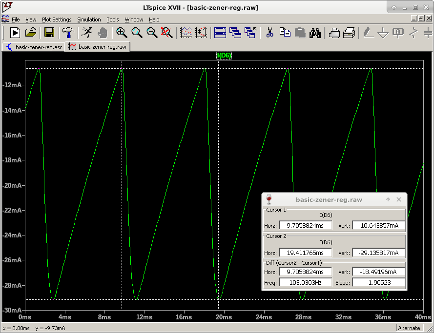
The datasheet uses 20mA as the test current, and lists the maximum allowed current as 55mA:

Screenshot_2020-10-01_00-17-58

In our circuit, the zener current varies between about 10 and 30mA, so we are averaging near 20 and are below 55mA:

Screenshot_2020-10-01_00-29-51

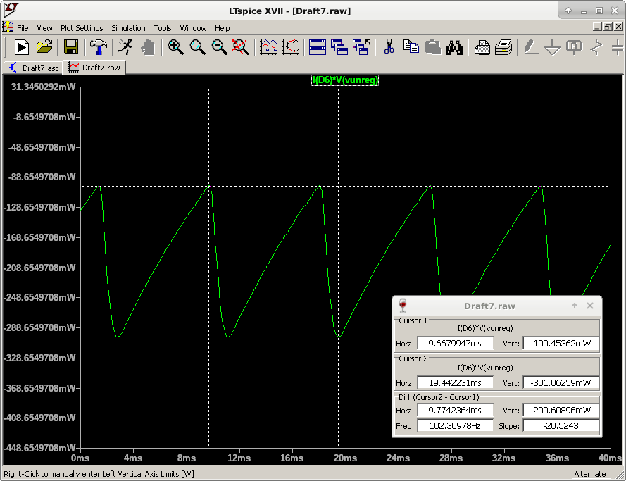
The 1N754 is a 500mW part, let's check the power dissipation. Select the plot window, then from the "Plot Settings" menu, select "Add trace". Type in I(D6)*V(vunreg) into the expression box:

Screenshot_2020-09-30_23-37-44

The power varies between 100 and 300mW, and it looks like the duty cycle is 50%, so the average power dissipation is 200mW, which is ok:

Screenshot_2020-09-30_23-40-48

Now let's push it out of regulation by increasing the current drawn by the load resistor:

  • Click the .op button and add a spice directive to step a parameter called RLOAD through a list of values: .step param RLOAD list 150 120 100 82
  • Right-click the Rload resistor and change its value to {RLOAD} (note the curly braces)

Screenshot_2020-10-01_00-06-47

Now we can see the zener progressively fall out of regulation by looking at Vz. As the load resistance gets lower, the load resistor draws more current, which pushed the zener out of regulation. The blue trace shows partial regulation, while the green trace is completely unregulated.

Screenshot_2020-10-01_00-07-52

We can also see this by looking at the current through the zener. Here, each progressively lower value of load resistance pushes the zener current closer to 0mA. The blue trace shows the zener current "clipping" at 0mA, falling in and out of regulation. The green trace is flat-lined at 0mA, indicating the zener has completely fallen out of regulation.

Screenshot_2020-10-01_00-25-23

Version 4
SHEET 1 3484 680
WIRE 352 48 96 48
WIRE 480 48 352 48
WIRE 528 48 480 48
WIRE 96 80 96 48
WIRE 96 80 -16 80
WIRE 224 80 96 80
WIRE -16 112 -16 80
WIRE 224 112 224 80
WIRE 480 112 480 48
WIRE 352 208 352 48
WIRE -16 240 -16 176
WIRE 64 240 -16 240
WIRE 224 240 224 176
WIRE 224 240 144 240
WIRE 480 240 480 192
WIRE 624 240 480 240
WIRE 672 240 624 240
WIRE 624 288 624 240
WIRE -16 304 -16 240
WIRE 224 304 224 240
WIRE 480 320 480 240
WIRE -16 400 -16 368
WIRE 96 400 -16 400
WIRE 224 400 224 368
WIRE 224 400 96 400
WIRE 96 432 96 400
WIRE 256 432 96 432
WIRE 352 432 352 272
WIRE 352 432 256 432
WIRE 480 432 480 384
WIRE 480 432 352 432
WIRE 624 432 624 368
WIRE 624 432 480 432
WIRE 256 464 256 432
FLAG 256 464 0
FLAG 528 48 Vunreg
FLAG 672 240 Vz
SYMBOL voltage 48 240 R270
WINDOW 0 32 56 VTop 2
WINDOW 3 -32 56 VBottom 2
WINDOW 123 0 0 Left 0
WINDOW 39 0 0 Left 0
SYMATTR InstName V1
SYMATTR Value SINE(0 12 60)
SYMBOL diode 0 368 R180
WINDOW 0 24 64 Left 2
WINDOW 3 24 0 Left 2
SYMATTR InstName D2
SYMATTR Value 1N4001
SYMBOL diode 0 176 R180
WINDOW 0 24 64 Left 2
WINDOW 3 24 0 Left 2
SYMATTR InstName D1
SYMATTR Value 1N4001
SYMBOL diode 240 176 R180
WINDOW 0 24 64 Left 2
WINDOW 3 24 0 Left 2
SYMATTR InstName D3
SYMATTR Value 1N4001
SYMBOL diode 240 368 R180
WINDOW 0 24 64 Left 2
WINDOW 3 24 0 Left 2
SYMATTR InstName D4
SYMATTR Value 1N4001
SYMBOL res 464 96 R0
SYMATTR InstName Rz
SYMATTR Value 47
SYMBOL cap 336 208 R0
SYMATTR InstName C1
SYMATTR Value 470�F
SYMBOL res 608 272 R0
SYMATTR InstName Rload
SYMATTR Value 150
SYMBOL zener 496 384 R180
WINDOW 0 24 64 Left 2
WINDOW 3 24 0 Left 2
SYMATTR InstName D6
SYMATTR Value 1N754
TEXT 320 504 Left 2 !.model 1N4001 D(Is=14.11n N=1.984 Rs=33.89m Ikf=94.81 Xti=3 Eg=1.11 Cjo=25.89p M=.44 Vj=.3245 Fc=.5 Bv=75 Ibv=10u Tt=5.7u Iave=1 Vpk=50 mfg=GI type=silicon)
TEXT -72 504 Left 2 !.tran 0 .05 .01 .000001
TEXT 320 472 Left 2 !.model 1N754 D(Is=1.616f Rs=1.818 Ikf=0 N=1 Xti=3 Eg=1.11 Cjo=120p M=.5117 Vj=.75 Fc=.5 Isr=1.698n Nr=2 Bv=6.8 Ibv=2.8814 Nbv=.28248 Ibvl=1.9426e-6 Nbvl=.27168 Tbv1=485.29u Vpk=6.8 mfg=Motorola type=zener)
Sign up for free to join this conversation on GitHub. Already have an account? Sign in to comment